Advancing High-Resolution, Responsible Patterning for Printed Electronics
23/04/2025As the demand for sustainable and high-performance electronics grows, so does the need for precise, low-waste manufacturing methods. A new research paper from our team explores two reverse-offset printing (ROP) approaches to create copper conductors with excellent resolution and minimal material usage — all on flexible substrates.
The study compares:
- Direct nanoparticle printing using copper ink combined with intense pulsed light (IPL) sintering
- Lift-off patterning of vacuum-deposited copper using a ROP-printed resist layer
Both techniques demonstrated impressive results:
- Less than 5% variation in conductor thickness and resistivity across large areas
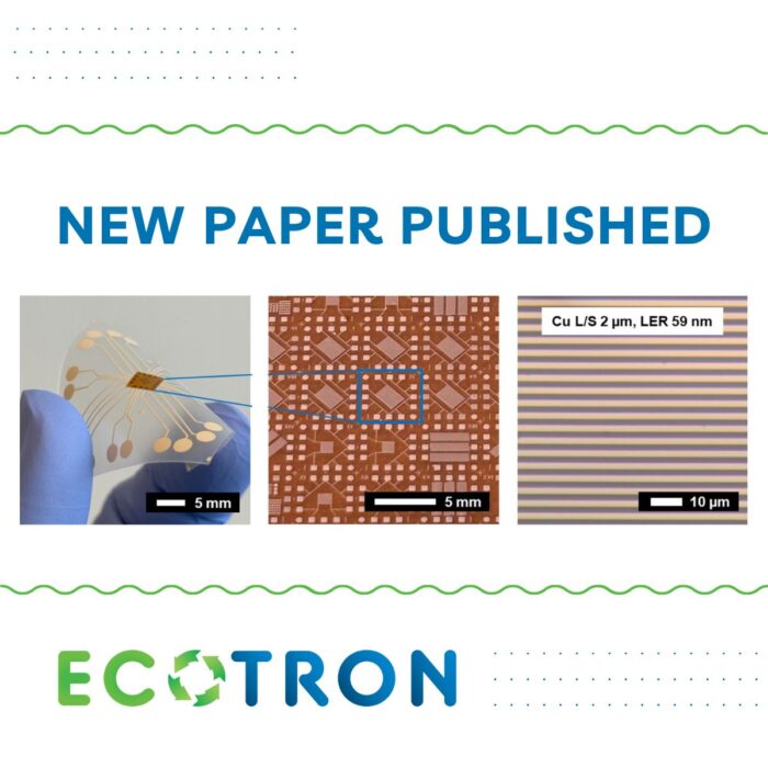
- 2 µm line-space resolution with low line edge roughness using the lift-off (LO) process
The research also showcases successful flexible chip assembly on stretchable substrates like TPU, with strong bending resistance — opening new possibilities for:
✔️ Wearable electronics
✔️ Environmental sensing platforms
✔️ Flexible and even biodegradable circuits
These advances reinforce the potential of ROP as a scalable and responsible patterning method in the printed electronics landscape.
Read the full paper here: Miniaturized Micrometer-Level Copper Wiring and Electrodes Based on Reverse-Offset Printing for Flexible Circuits | ACS Applied Electronic Materials